
You are using an out of date browser. It may not display this or other websites correctly.
You should upgrade or use an alternative browser.
You should upgrade or use an alternative browser.
-
You can now help support WorldwideDX when you shop on Amazon at no additional cost to you! Simply follow this Shop on Amazon link first and a portion of any purchase is sent to WorldwideDX to help with site costs.
CPI 2000 issues
- Thread starter Danzik
- Start date
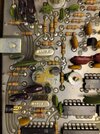
From the position close to the two crystals I'm going to have to guess that one is either C646 (.1 uFd) or C647 (5 pF) and the other is either C637 (.01 uFd) or C649 (5 pF).
Unfortunately no one has ever taken the time to produce a Sam's like diagram with arrows to each part on a photo of the board and I haven't spent enough time inside one of these to be able to tell you for sure.
Gregg at s9radio might know. I pulled his email address from YouTube:
s9radio@aol.com
Unfortunately no one has ever taken the time to produce a Sam's like diagram with arrows to each part on a photo of the board and I haven't spent enough time inside one of these to be able to tell you for sure.
Gregg at s9radio might know. I pulled his email address from YouTube:
s9radio@aol.com

Hi, Gregg did get back with me and stated that there really isn't a exact set value of capacitor for these two areas but he said it is usually between 1-5 pf ,he said what I am doing is called padding the crystals to get it to where the two pots will adjust right to the correct frequencies. He did also say it is recommended to use NPO or CGO style capacitors so they don't not change value due to temperature changes.From the position close to the two crystals I'm going to have to guess that one is either C646 (.1 uFd) or C647 (5 pF) and the other is either C637 (.01 uFd) or C649 (5 pF).
Unfortunately no one has ever taken the time to produce a Sam's like diagram with arrows to each part on a photo of the board and I haven't spent enough time inside one of these to be able to tell you for sure.
Gregg at s9radio might know. I pulled his email address from YouTube:
s9radio@aol.com
I am somewhat concerned now to why they were removed in the first place though, perhaps someone went to do a alignment on the radio and couldn't get it on frequency and there could be somthing else wrong, we'll find out in due time I guess
Hi, I did try a couple caps in the vacant locations and it did not seem to make any difference at all. I do know that there is not any voltage changes on the outputs of the chip that I have the red pointer on when changing the channels, should there be ? I am guessing so. When I got this radio someone had a wire going from the 2 pins on that chip that has solder that looks disturbed and the wire was going back to the noise blanker switch and when turned on it sounded like the NB was working correctly, however I removed the wire and hooked the switch back up like it would have been originally and now the noise blanker also appears to be working fine, so I am not sure why someone attempted that modification but it is questionable to me if this chip is working correctly
.
.

Looks like a 10 kc mod. Tie the constant +5v on pin 1 to bit 1 input on pin 3.
That chip is the first stage of the programmable divider. So altering that first bit will drive radio up or down 10 kc.
Should have a signal in on pin 2 and signals out on pins 11, 12, 13, 14, and 15. The programmable divider is set by the values on pins 3, 4, 5, and 6.
The chip itself is a 74160 BCD counter. According to the schematic I have you could also substitute a Fairchild 9310 if no 74160 chips are available.
These here would work wouldn't they TM86?Looks like a 10 kc mod. Tie the constant +5v on pin 1 to bit 1 input on pin 3.
That chip is the first stage of the programmable divider. So altering that first bit will drive radio up or down 10 kc.
Should have a signal in on pin 2 and signals out on pins 11, 12, 13, 14, and 15. The programmable divider is set by the values on pins 3, 4, 5, and 6.
The chip itself is a 74160 BCD counter. According to the schematic I have you could also substitute a Fairchild 9310 if no 74160 chips are available.

Should, it's the same part number as what you've got in the radio right now.These here would work wouldn't they TM86?View attachment 75156
I ordered about 4 of them since I have heard they run hot anyways, the shipping was more than the chip itself so might as well get extrasShould, it's the same part number as what you've got in the radio right now.
Every once in a while I get too involved when I should be sleeping.
I see a problem with the schematic. . . .
The IC (74160 G) that you took the switch wires off, "pin 3" is shown on the schematic as going to "pin 11" of the PLL, but that fine picture that you took of the bottom traces shows "pin 3" as being held low by a resistor (2.2K) that goes to ground. "Pin 11" is being held low by a 6.8K resistor going to ground.
(Just wondering what would happen if it was wired per the schematic, pin 3 to 11 to let the PLL control pin 3? )
On the PLL (U700N / MM 5221) pins 4~11 are output pins that feed the two 74160 "G" and "H".
You may be looking at it wrong if you think the 74160 (H&G) controls the PLL, they go to the Phase Detector circuit. Their are many wave forms on that schematic that should help you trace those IC chips with a scope.
The channel selector switch connections (as shown on the schematic) go to
pins 21, 1, 2, 3, 19, 18, & 20 of the PLL.
If you do decide to replace that IC (74160), clip all the pins so that you can unsolder them separately. Do not clip them short leave as much pin material to be able to hold on to them while unsoldering.
Good luck, looks interesting ......
Thank you Dr. Frankenstein but you know alot more about this then I actually do I can tell. One thing though as far as the schematic goes I know there were 2 different cp 2000 boards the older one and a newer one and I have the newer one and I am thinking the schematic was for the older one as I see alot of resistor values look different the the schematic in mine. I do not have the radio in front of me right now but I will definitely be looking at what you said about the pin 3. Thank you much !Every once in a while I get too involved when I should be sleeping.
I see a problem with the schematic. . . .
The IC (74160 G) that you took the switch wires off, "pin 3" is shown on the schematic as going to "pin 11" of the PLL, but that fine picture that you took of the bottom traces shows "pin 3" as being held low by a resistor (2.2K) that goes to ground. "Pin 11" is being held low by a 6.8K resistor going to ground.
(Just wondering what would happen if it was wired per the schematic, pin 3 to 11 to let the PLL control pin 3? )
On the PLL (U700N / MM 5221) pins 4~11 are output pins that feed the two 74160 "G" and "H".
You may be looking at it wrong if you think the 74160 (H&G) controls the PLL, they go to the Phase Detector circuit. Their are many wave forms on that schematic that should help you trace those IC chips with a scope.
The channel selector switch connections (as shown on the schematic) go to
pins 21, 1, 2, 3, 19, 18, & 20 of the PLL.
If you do decide to replace that IC (74160), clip all the pins so that you can unsolder them separately. Do not clip them short leave as much pin material to be able to hold on to them while unsoldering.
Good luck, looks interesting ......
"Rubbering" a crystal.padding the crystals
"Rubbering" a crystal in electronics, especially amateur radio (
QRP), refers to making small frequency adjustments to a crystal oscillator, usually by adding a variable capacitor or varactor diode in series or parallel with the crystal to "pull" or fine-tune its operating frequency slightly, allowing for minor shifts for better tuning or to avoid interference. It's a common technique in simple transceivers, sometimes called a VXO (Variable Crystal Oscillator) when a variable capacitor is used, enabling flexibility without replacing the crystal.
A crystal can also be pushed via series inductance. Ask the TRC449, 457/458 synthesizer how that works.
And of archaic note, The crystal itself could be removed from a ft243 holder and manipulated in curious ways to alter the frequency and then replaced in the holder.
And for you crayon munchers, here's the video
Thanks for looking out for us.And for you crayon munchers, here's the video
If you replace any of the ICs, solder a socket to the board to insert the IC into. This way, you will never have to do any soldering at those points again if the replacement IC needs to be removed again. This prevents damage to the traces and from over heating of the IC while soldering.
dxChat
- No one is chatting at the moment.
-
@ Hambones amps:Does anyone know if you can replace the 2290 in a galaxy dx 93t twin turbine with a 2sc2879 red dot? If so, what would have to be tuned?
-
-
@ ShadowDelaware:Hambones the entire amp section would have to be retuned, and the rf transformers re wrapped.
-