• You can now help support WorldwideDX when you shop on Amazon at no additional cost to you! Simply follow this Shop on Amazon link first and a portion of any purchase is sent to WorldwideDX to help with site costs.
  • A Winner has been selected for the 2025 Radioddity Cyber Monday giveaway! Click Here to see who won!

Another Saturn bias issue

Hawkeye351

Sr. Member
Jun 27, 2021
800
752
103
58
Got another Galaxy Saturn on the desk today.

Issue:
Keeps blowing finals.

Evaluation:
Passthrough regulator is fine.
AF regulator is fine.
Pre-driver is fine.
Driver is fine.
Replaced both finals with good ones.
No swing mods.
Output caps test as good.
All traces have firm joints.
Bias diodes across driver/finals test good.
Both final bias VR adjustments replaced.
Driver bias adjustment tests as fine.
Resistors in bias section look good, and test as fine.
Bias Inductors look and test as good.

With all driver/final leads soldered to their respective pads, I get 0.037 ohms resistance when probing the emitter and base of the finals, but I get around .654 ohms when probing the emitter and base of the driver.

If I lift the collector of all three and probe emitter to base of all three again, same result.

That's with meter in 200/speaker mode not diode mode. Flip the meter into diode mode and they check out as they should.

With everything hooked up, the driver pulls 50ma without even turning it's bias VR off the zero spot. The first final pulls 500ma with bias VR all the way down to zero, both the first and last final both pull around 984ma with both bias VR adjustments turned all the way down.

100 ohm variables for finals, 1000 ohm variable for driver. All three test well within range.

Receive and everything else works great on this rig, just the output stage drawing too much current without any bias adjustment on any of the three bias adjustment VR's.
 

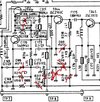
if the bias is way high, just the diodes D112/088 could be conducting
at a lower voltage. I pull all that stuff off. and remake the bias circuit
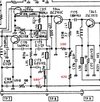
like this diagram. I also changed an old "orange face" 2950 to have
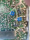
a circuit like this, and I glued some 1k pots on the bottom of the board.

parts to remove.jpg

..... make it look like this

new bias circuit.jpg

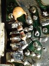
100 ohm R at driver.jpg

....

2950 bias addition    2.jpg

a 2950 with a new adjustable bias circuit, for the finals.
works great now....
 
here is the post.
from just several months ago.
But I have changed the bias circuit on several of these types of radios.

 
  • Like
Reactions: Hawkeye351
Hmmm, never seen this before:
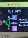
NPN BJT tests as a good BJT NPN but notice the diode from collector to emitter on test result screen?

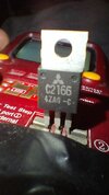
2SC2166

IMG_20251211_171439009.jpg
 
Last edited:
Hmmm, just tested 4 other 2166's that I had in the parts box (used), and all of these show that diode symbol across the collector to emitter. But my 2078, 2092, 1969, 2312 transistors don't show that diode symbol between C and E.

Maybe all my parts 2166 that I yanked out of old radios is shot also, just seems odd.

Is it normal for a 2166 to show a diode symbol between C and E on a tester but not other BJT NPN transistors?
 
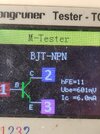
Mine shows that too, but in the form of a little p after NPN. Chatgpt says this transistor was from the germanium-silicon transition era and some had the protection diode added as an overvoltage clamp in RF stages.
20251212_005110.jpg
20251212_005138.jpg
 
  • Like
Reactions: Hawkeye351
Oh, I learn something every day, lol...

I think all my 2166's are flat anyway. Highest HFe I can find is a 21 which is well below the minimum point for a 2166. I've got plenty of 2078' 2029, 2092, etc... but no more 2166. Gotta figure something out.

Would a very low hfe cause a high current draw? Can't figure out why the bias is so high with no bias adjusted.
 
Can't figure out why the bias is so high with no bias adjusted.
if those MV1Y diodes start conducting at a higher voltage,
above .7V, or go open, then you may have trouble adjusting
the bias current down, and the base current may be so high
that the transistor blows out.

you could put some 1N4148's in place of them MV1Y's.
just solder them under the board. and check your
bias current results. just try your 2166 driver at first.

I remove all that, and change the bias circuit, to a
reliable and predictable circuit using only resistors,
since there is a regulated 8V supply to this bias circuit.
 
I'm gonna try the bias circuit changes on one of my personal Saturns after I'm done with this one. The guy wants it stock, therefore I can't tinker with the bias circuit on this one.

I finally did run across a good Mitsubishi 2166 though, after going through a dozen or more I finally got one with a good HFe. Had to yank it out of one of my personal old school 1st gen 2950's I use for parts. Got an HFe of 47. Minimum HFe for a Mitsubishi 2166 is listed as 35, typical being 50 so I think this 47 HFe should would good.

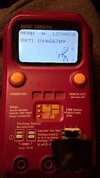
And yes, this good one also shows the diode symbol across the collector to emitter. Odd thing is, I also have a newer FNRSI component tester that doesn't show that collector to emitter diode symbol, but it does show lower HFe figures. The TC1 shows that symbol on 2166's, but not other drivers/finals.

Gonna try this driver and get back with y'all. Thank you all for popping in.
 
I've never owned the one you have, so I don't know which is better. This is the first and only component tester I have had.

Is it possible there is a blocking cap between the driver and finals leaking?
 
Thought of that myself and yanked all the disc caps out of the RF section to check. All check good and very close to their respective values.

Gonna put all these back in, then look over very closely with bench mag glass to check for any cracked traces or bodged joints. I guess I will try it out if everything looks good.
 

dxChat
Help Users
  • No one is chatting at the moment.