Various channels are off by 40kHz, if my math is right.
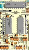
This is the 690011D board like the dx959 and 98vhp, not like the old 99v 3600 board.
The following channels read 40,000hz high. Example: 36=27.4050 instead of 27.3650
1.5,6,7,12,13,18,19,20,23,26,27,28,33,34,35,36.
The only channels that are on frequency are 2,3,3,8,9,10,11,14,15,16,17,21,22,24,25,29,20,31,32,37,38,39,40.
*Channel 20
TP3 = 16.5500 instead of 16.5100
*Ant Jack @ 27.2450
Before getting too deap, maybe someone knows what’s wrong just by the above info.
Alignment of PLL done according to 98vhp.
Note: 99V2 has a vr5 and 98vhp does not.


")