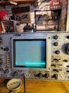
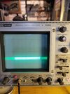
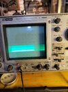
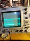
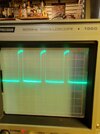
Like I have said I really don't know what I am doing with the scope yet for sure, but Nomad helped quite a bit here, I turned down sweep time/ div to 2 and put the probe on pin 2 on that ic I had replaced and the line rises but I really don't think it really shows a waveform I don't know. The first picture is with the probe off and I had set the line to 0% at the bottom. The second photo is with the probe on pin 2. Perhaps I need to make adjustmentsIf you have an oscilloscope you should see a waveform on pin 2, not just a DC voltage.

You are using an out of date browser. It may not display this or other websites correctly.
You should upgrade or use an alternative browser.
You should upgrade or use an alternative browser.
-
You can now help support WorldwideDX when you shop on Amazon at no additional cost to you! Simply follow this Shop on Amazon link first and a portion of any purchase is sent to WorldwideDX to help with site costs.
-
A Winner has been chosen for the 2026 July 4th Retevis RA89R Giveaway! Click Here to see who won!
CPI 2000 issues
- Thread starter Danzik
- Start date
From what I can see you do have a signal on pin 2. I just can't say if it's any good or not. It should be in the neighborhood of 4 MHz or so. Or at least that's what the service manual says.
I went back in the thread and found where the schematic and some service notes were uploaded, but not the service manual, so I'm attaching that here. It can probably answer your questions faster and more accurately than I can.
I went back in the thread and found where the schematic and some service notes were uploaded, but not the service manual, so I'm attaching that here. It can probably answer your questions faster and more accurately than I can.
Attachments

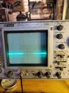
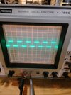
Forgive my ignorance as I have never had the pleasure of owning an analog scope (cool!), but what is with the bright and dark bands? Is that persistence from the phosphor or a camera artifact?
Why not adjust the horizontal scale a little to try to see the rise and fall of the actual signal? It is clear there is an AC signal there, but it is not clear what it is.
1/frequency=cycle period. If you expect to see a 4MHz signal, set the time per division close to that period so you can see whats happening.
Did you calibrate your new probes?
Yeah, I am new to using a scope and I need to work with it a bit and do some research in them, I will try your adjustments and also look into how to calibrate the probes because no I did not calibrate them yet. Thank you for the advice I appreciate it, this is a new ordeal for meForgive my ignorance as I have never had the pleasure of owning an analog scope (cool!), but what is with the bright and dark bands? Is that persistence from the phosphor or a camera artifact?
Why not adjust the horizontal scale a little to try to see the rise and fall of the actual signal? It is clear there is an AC signal there, but it is not clear what it is.
1/frequency=cycle period. If you expect to see a 4MHz signal, set the time per division close to that period so you can see whats happening.
Did you calibrate your new probes?
The dot scans from left to right at a rate that makes audio signals legible. An RF waveform naturally moves up and down way too fast to separate the ups and downs of the waveform. Makes the "luminous band" trace this way. Naturally if you speed up the horizontal time base to a microsecond or (typically) less, the actual RF waveform becomes visible. But anything with a lower frequency now gets stretched from left to right as a barely tilted flat line.
Rolling the time base knob up and down will reveal the tradeoff between seeing low-frequency stuff a one end, and the actual RF waveform at the other end of the knob's travel.
73
Rolling the time base knob up and down will reveal the tradeoff between seeing low-frequency stuff a one end, and the actual RF waveform at the other end of the knob's travel.
73
Hi Nomad thanks for the reply, I think you were correct about the age of the scope though and I do not think it is operating properly. I did take the cover off today and cleaned the volts/ div as well as I could and it did help, I went to calibrate the probe and you can barely see the vertical lines on the screen " pic" however when I touch the probe with my finger I get some action that looks normalThe dot scans from left to right at a rate that makes audio signals legible. An RF waveform naturally moves up and down way too fast to separate the ups and downs of the waveform. Makes the "luminous band" trace this way. Naturally if you speed up the horizontal time base to a microsecond or (typically) less, the actual RF waveform becomes visible. But anything with a lower frequency now gets stretched from left to right as a barely tilted flat line.
Rolling the time base knob up and down will reveal the tradeoff between seeing low-frequency stuff a one end, and the actual RF waveform at the other end of the knob's travel.
73
Attachments
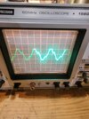
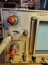
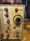
Hi, Thanks for your reply, I have adjusted just about everything on this scope when it comes to getting a waveform from the radio and all I get is a blotch of green, I have messed with the sweep time / div and volts div with no success, I did get the probes calibrated I believe. Here are photos of the scope settings I have at the moment if you see anything wrong please let me know. ThanksForgive my ignorance as I have never had the pleasure of owning an analog scope (cool!), but what is with the bright and dark bands? Is that persistence from the phosphor or a camera artifact?
Why not adjust the horizontal scale a little to try to see the rise and fall of the actual signal? It is clear there is an AC signal there, but it is not clear what it is.
1/frequency=cycle period. If you expect to see a 4MHz signal, set the time per division close to that period so you can see whats happening.
Did you calibrate your new probes?
Attachments
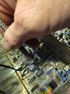
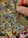
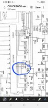
Yeah, I see that too ! Yeah pin 11 of the pll is clearly not going all the way to pin 3 of the divider but it shows it in the schematic? Hmmm anyone else know anything about that ?Every once in a while I get too involved when I should be sleeping.
I see a problem with the schematic. . . .
The IC (74160 G) that you took the switch wires off, "pin 3" is shown on the schematic as going to "pin 11" of the PLL, but that fine picture that you took of the bottom traces shows "pin 3" as being held low by a resistor (2.2K) that goes to ground. "Pin 11" is being held low by a 6.8K resistor going to ground.
(Just wondering what would happen if it was wired per the schematic, pin 3 to 11 to let the PLL control pin 3? )
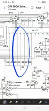
On the PLL (U700N / MM 5221) pins 4~11 are output pins that feed the two 74160 "G" and "H".
You may be looking at it wrong if you think the 74160 (H&G) controls the PLL, they go to the Phase Detector circuit. Their are many wave forms on that schematic that should help you trace those IC chips with a scope.
The channel selector switch connections (as shown on the schematic) go to
pins 21, 1, 2, 3, 19, 18, & 20 of the PLL.
If you do decide to replace that IC (74160), clip all the pins so that you can unsolder them separately. Do not clip them short leave as much pin material to be able to hold on to them while unsoldering.
Good luck, looks interesting ......
Attachments
Got a new toy for Christmas and yes pin 2 looks real close to 4 MHzFrom what I can see you do have a signal on pin 2. I just can't say if it's any good or not. It should be in the neighborhood of 4 MHz or so. Or at least that's what the service manual says.
I went back in the thread and found where the schematic and some service notes were uploaded, but not the service manual, so I'm attaching that here. It can probably answer your questions faster and more accurately than I can.

dxChat
- No one is chatting at the moment.
-
-
-
@ BJ radionut:Scheduled for Jul 4, 2026 Saturday Live Streams:
To celebrate the 250th birthday of our great nation. We are giving away not just one, but multiple antennas! The Grand prize is the CaHR-Tenna Hydra Antenna, along with several other antenna prizes that will be announced throughout the giveaway. Whether you're a new ham, portable operator, POTA activator, or an experienced HF operator, this is your chance to upgrade your station. Prizes Include: HRA Hydra Antenna (Grand Prize) Additional antennas from HRA More prizes may be added during the giveaway! -
-
