• You can now help support WorldwideDX when you shop on Amazon at no additional cost to you! Simply follow this Shop on Amazon link first and a portion of any purchase is sent to WorldwideDX to help with site costs.

EPT360015C Connex cx3400hp dual mosfet issue.

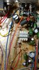
Driver gate voltage pad (on board)
Down - 1.58v
Middle - 5.91v
Up - 6.80v

Adjustment is very smooth, no sudden increases, decreases, drops, etc...

1st final gate voltage pad (on board)
Down - 0.00v
Middle - 3.38v
Up - 4.25v

Same adjustment results as driver, very smooth transition from low to high.

Last final gate voltage pad (on board)
Down - 0.00v
Middle - 3.43v
Up - 4.35v

Same adjustment result as 1st final and driver, very smooth transition from low to high.

Note: The AM power adjustment (variable power on the board) is turned as low as it will go, if I increase it then the gate voltage on the driver gate pad increases from 5.97v to 6.41v with the driver trimmer set to middle (as noted at the top of this message).

Still no heating issues and hardly any current draw on my power supply meter.
 
Note: The AM power adjustment (variable power on the board) is turned as low as it will go, if I increase it then the gate voltage on the driver gate pad increases from 5.97v to 6.41v with the driver trimmer set to middle (as noted at the top of this message).

Can you spare a pic of top and bottom of that section - sounds like a mod is still present - the AM power should not affect Gate BIAS. The Pic is to help me see if there is something more that if we were to continue, will wreck your recovery efforts...

It could also be a component that failed.

One last comment...

The Diodes your using - are they Zener or standard diode?

Why do I ask - because the GATE of the DRIVER would not have gone up over 5 volts - the Zener would have clamped it to keep it steady at the "zener voltage", it's rated for. (Unless you bought Zeners that are the 7.5V ones which would explain this) As long as you're seeing adjustable voltage that stays where you put it - is the result we need. So ... about the voltage Driver needs work - we need to fix the AM power feeder line or locate the potential short so it's not adding BIAS we're trying to keep under control.

The Zener can be damaged - or you're using the wrong part.

This "event" could explain why the Driver failed so easily.

This is from a 959 board, but I'm leaving it here "colorized" to help you sort out and possibly locate the potential short thru the traces outline and some traces are the same color - while others are thier own color but repeated between the driver and final section - we have to somehow fix the Bias so the BIAS areas are colored to help you in sorting this out.

upload_2021-11-18_17-42-19.png

I'm also enclosing a schematic of a 959 which is the SINGLE final of an 86V - but you can use this as a template to help you in identifying the foil side and the component sides.
upload_2021-11-18_17-51-45.png
 
Last edited:
Top side back left corner over to output section:
1118211812.jpg

Driver final side top view:
1118211812a.jpg

Bottom side:
1118211816_HDR.jpg

1118211815_HDR.jpg

Zoomed in on 2 diode locations with 2 diodes tied together on each:
1118211813.jpg

1118211814.jpg
 

Attachments

  • 1118211812b.jpg
    1118211812b.jpg
    1.7 MB · Views: 4
  • 1118211813_HDR.jpg
    1118211813_HDR.jpg
    1.6 MB · Views: 3
  • 1118211813a_HDR.jpg
    1118211813a_HDR.jpg
    1.6 MB · Views: 3
Ok, just to prepare you...

There is an error - but nothing we can't fix...

Here's why...

Look at your Driver on the FOIL side...

upload_2021-11-18_18-50-29.png

Each one of the Driver and Final "sections" have two notches.

This is where the Diode goes into - those "slots" from the top of the board and are nestled in just under the MOSFET.

They only go in one way - see above - but the part - the diode Zener - the Banded end is to the RIGHT in the picture - so this is the rear panel view...

The Same applies to the Finals.

You're doing great - keep going!
 
Here's a tip...
from another board similar to yours...a dual final type using MOSFET...
upload_2021-11-18_19-0-10.png

See the Arrows? they slide in and under the MOSFET they protect - and the banding in this pic - is to the LEFT on the component side.
 
  • Like
Reactions: NZ8N
ON another note...

I wanted to compliment you on the work you're doing...

upload_2021-11-18_19-24-26.png
I noticed something several tech I worked around in a former job, often forgot to do...

Mount the part but remember to SOLDER a leg - usually the SOURCE (Emitter in Bipolar) to ground to help reduce static potential damages...

You're following and doing the right procedures as far as I can tell from here....

Thank you for for letting me work alongside.


Keep going!
 
Last edited:
Is there some solder cleanup I gotta do on the final pads or diode slot locations? Do I have a trace or two soldered together by mistake?

The diodes were mounted on the bottom of the board, along with a 104 disc capacitor on each one separately (3 mosfets, 3 diodes, 3 disc caps). He told me the mosfets had been replaced before and that talk back mod installed, which I removed.

Only things I did were:
Replaced 2sb827 with a tip36c
(2sb827 had a hole blown in it)
Replaced both 1819s with 2sa1012s
Replaced the mosfets
(the driver mosfet had a hole blown in it)
Removed the talkback mod
Rebiased
Tuned (even RF Stage)
Everything went great after I got that tone out of the carrier, but the regulator heat issue and slack on wattage is got me stumped.

Thank you for the compliment on my work, I always thought my solder work was sloppy.
 
Andy, should I put those diodes back in circuit and test the driver gate voltage pad again? And if yes, then should I also put those 104 caps back on the diodes? Still with mosfets unsoldered from the board?
 
Ok, you're asking some good questions, mostly regarding with Assembly - which is the REAL effort.

Ok, I've searched thru the photos and I still am, but also remember too - I don't have the board you're working on in front of me to visually check the work and progress. I see others work in there which makes this more challenging because you have to "undo" the mistakes of the former - recreate the original problem, then fix that - then proceed to repair replace and tune up to get it back into the customers hands.

You're not in any way in bad shape, you're really doing quite well considering this is new to you.

You're patience is wonderful to deal with - we've had posters out here on the 'net - that if they didn't get an answer within say; an hour, they're throwing out the radio into a firepit...

Ok, I'm still concerned about the DRIVER section and it's Gate bias going up and down with AM power. I can't see anything directly - but the soldering in some areas does need to be cleaned up - reflowed with some even removed to help with the "mounds" to make the traces appear correctly soldered.

The only thing I may have an answer to, is for why the DRIVER BIAS goes up and down with AM Regulation.

You have a small "hairline" solder bridge - potential short - just clean it up and see if the AM power doesn't keep showing up on the Gate Bias or the GATE solder pad itself.

See below...
upload_2021-11-19_7-37-48.png

The coil in front is for the DRAIN power from the AM Regulator.
There is also a Jumper J41 the heads off to the Final pair.
The "10K" Resistor feeds the BIAS to the Gate from the Trimmer.
All part are correctly placed, just the possible solder bridge.​

So just "wick up" those two pads, Gate and Drain - then recheck to make sure the AM Regulator power goes up and down and doesn't affect GATE.
 
  • Like
Reactions: NZ8N and Hawkeye351
Andy, should I put those diodes back in circuit and test the driver gate voltage pad again? And if yes, then should I also put those 104 caps back on the diodes? Still with mosfets unsoldered from the board?

Had to put the discovery priority first - then this to reply to answer.

Right now, keep the diodes out so you lessen the risk - we have to verify the Gate is GATE powered by GATE Bias not AM REGULATOR getting included...

Then once BIAS is stable - go ahead and continue the reassembly...

The 104's do need to go back on the DIODES - this is so they can keep DC and get RF out of the BIAS circuit and like with the AM Regulator - keep RF and BIAS separated. RF - belongs to the MOSFETS' respective leads not their BIAS.

I also ask that you remember to keep J41 clear of the diode package - I have witnessed several problems around the Notch and J41 - getting too close in clearance causing problems.
 
Last edited:
I'll get to that in the morning. Sorry to be in and out on this but daily duties hold me up. I spoke to the guy and asked him to give me just another week or so and he's ok with that.

Thank you so much Andy for hanging in there with me, I truly appreciate all you're doing, and keeping notes too for future reference.
 
  • Like
Reactions: Handy Andy
Ok, I wicked out the driver and finals pads. Looks good to me. The variable power (on the board) is no longer affecting the gate voltage on the driver gate pad, but the gate voltage on that driver gate pad won't go any lower than 2.45v now. It will go as high as 6.45v.

Here is a current photo of my wick cleanup.
1121211637_HDR.jpg
 

dxChat
Help Users
  • No one is chatting at the moment.