This radio does RX and transmit and has audio but the power is less than a watt. Driver bias is very high 8.31 - 8.48 volts and won't adjust beyond these numbers. The VR 11, driver, Finals, Zeners, pre driver, IC 4, Audio Amp TR51, Have been replaced. I have voltage tested every Transistor and IC on the board and all are very close to the voltage chart from CBC International. I started my first radio repair 6 weeks ago. I am learning and would really appreciate some guidance here. Thanks in advance. This site has helped me plenty just by reading old discussions.
You are using an out of date browser. It may not display this or other websites correctly.
You should upgrade or use an alternative browser.
You should upgrade or use an alternative browser.
-
You can now help support WorldwideDX when you shop on Amazon at no additional cost to you! Simply follow this Shop on Amazon link first and a portion of any purchase is sent to WorldwideDX to help with site costs.
Saturn EPT360014B
- Thread starter QuickdrawMcgraw
- Start date
What is bias current for driver and final(s)? Is it adjusting?
Are you sure driver/final transistor is legit? Have you verified that? So many counterfeit around.
Are you sure driver/final transistor is legit? Have you verified that? So many counterfeit around.
The radio has been upgraded to mosfet’s,They are legit bought from Mouser. Problem is I assumed the driver and finals were bad, my mistake. The Bias for the finals is perfect 3.6 volts the driver will only adjust from 8.4 to 8.3 volts. The pot is 100k. And has been replaced and double checked.What is bias current for driver and final(s)? Is it adjusting?
Are you sure driver/final transistor is legit? Have you verified that? So many counterfeit around.
I will measure the current and post it later today. Sorry!What is bias current for driver and final(s)? Is it adjusting?
Are you sure driver/final transistor is legit? Have you verified that? So many counterfeit around.
So there s something wrong with driver circuit. Since it is converted, I can't tell what it is.
Mike
Mike
The driver current is 10.45 amps yes 10.45 whole amps. The finals combined current is 100ma.What is bias current for driver and final(s)? Is it adjusting?
Are you sure driver/final transistor is legit? Have you verified that? So many counterfeit around.
Nothing is shorted. The driver transistor checks good out of the radio. It’s probably something really dumb.
What’s your armchair diagnosis if it’s not converted?So there s something wrong with driver circuit. Since it is converted, I can't tell what it is.
Mike
Not converted radio:
1. Faulty MV1Y diode. You can use 1n4148 as replacement.
2. Bad/counterfit transistor.
3. Bad potentiometer
4. Bad resistor in bias circuit.
5. Cold solder joints.
In that order.
Mike
1. Faulty MV1Y diode. You can use 1n4148 as replacement.
2. Bad/counterfit transistor.
3. Bad potentiometer
4. Bad resistor in bias circuit.
5. Cold solder joints.
In that order.
Mike
The MOSFET is missing the Bias Source to Drain - resistor network.
They are not Bipolars, that type needs an MV-1Y or a typical 1N4148 PN diode (Read as: Non-Schottky)
These guys, your MOSFET need a source resistor, and a dropping resistor - two resistors from the 8V bias line - the middle where the two resistors meet, is the Bias point - a resistor divider with the middle connection being towards the GATE or with that 100K trim, you shunt the output wiper arm - load across it, with a 47K resistor (or 4.7K if they did the Final Bias too - just duplicate that if you can) to that same GATE.
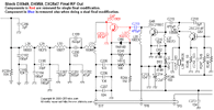
After
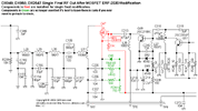
See the Green highlighted work? You rework the DRIVER side and source thru that
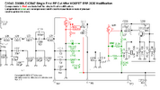
So D92 gets pulled, L37 can be kept - R245 changed to a 47K and at junction of R245 and D93 (D93 is removed - kept for later to be installed elsewhere)
The Trace where D93, R246 and VR12 meet you install a 39K resistor from that junction trace, solder 1 leg to that trace and across to foil ground the other resistor leg gets soldered to that foil ground.
Thats the Divider for the voltage trimmer.
VR12 then sources 1/3 the supply rail voltage to turn on the MOSFET
But you're not done, then at the junction of where D92 went solder a 2.2K resistor and D93 or D92 either or can be used, as the Bias diode and resistor (done in series) to drop 1/5 the output of VR12 - so this should give you an adjustment of 2.3 to as much as 3.4 volts - which is all you need for the Driver.
You see two dividers, yes that is correct, and the reasoning is the DC side, is the HIGH-IMPEDANCE side which gives you your source voltage to start.
The other side, towards the Driver itself, is the secondary one that handles RF issues when RF is present in higher amounts that can get "reinjected" so the purpose of the D92 is to rectify that RF into a DC-current you can work with in the RF - Driver side.
The Diodes BANDED end goes towards Foil Ground.
Some people revert to the older style of Zener across where D92 was, D93 if it exists - is removed.
What you have to keep in mind, if you decide to do this, is if you go the Zener route, that diode can get your biasing into trouble - you can shoot more voltage to the MOSFET - latching it on - as you're experiencing now.
So you'll have to "divide" down the voltage to less than 4V and adjustable from 2.5 to 4.1 volts - to make this work.
10 Amps is not correct - 100mA or even 55mA is the recommended draw.
Attached is a PDF I captured from the old CB Tricks site to show how to convert the older "dual final 2312 - style" EPT3600 boards.
They are not Bipolars, that type needs an MV-1Y or a typical 1N4148 PN diode (Read as: Non-Schottky)
These guys, your MOSFET need a source resistor, and a dropping resistor - two resistors from the 8V bias line - the middle where the two resistors meet, is the Bias point - a resistor divider with the middle connection being towards the GATE or with that 100K trim, you shunt the output wiper arm - load across it, with a 47K resistor (or 4.7K if they did the Final Bias too - just duplicate that if you can) to that same GATE.

After

See the Green highlighted work? You rework the DRIVER side and source thru that

So D92 gets pulled, L37 can be kept - R245 changed to a 47K and at junction of R245 and D93 (D93 is removed - kept for later to be installed elsewhere)
The Trace where D93, R246 and VR12 meet you install a 39K resistor from that junction trace, solder 1 leg to that trace and across to foil ground the other resistor leg gets soldered to that foil ground.
Thats the Divider for the voltage trimmer.
VR12 then sources 1/3 the supply rail voltage to turn on the MOSFET
But you're not done, then at the junction of where D92 went solder a 2.2K resistor and D93 or D92 either or can be used, as the Bias diode and resistor (done in series) to drop 1/5 the output of VR12 - so this should give you an adjustment of 2.3 to as much as 3.4 volts - which is all you need for the Driver.
You see two dividers, yes that is correct, and the reasoning is the DC side, is the HIGH-IMPEDANCE side which gives you your source voltage to start.
The other side, towards the Driver itself, is the secondary one that handles RF issues when RF is present in higher amounts that can get "reinjected" so the purpose of the D92 is to rectify that RF into a DC-current you can work with in the RF - Driver side.
The Diodes BANDED end goes towards Foil Ground.
Some people revert to the older style of Zener across where D92 was, D93 if it exists - is removed.
What you have to keep in mind, if you decide to do this, is if you go the Zener route, that diode can get your biasing into trouble - you can shoot more voltage to the MOSFET - latching it on - as you're experiencing now.
So you'll have to "divide" down the voltage to less than 4V and adjustable from 2.5 to 4.1 volts - to make this work.
10 Amps is not correct - 100mA or even 55mA is the recommended draw.
Attached is a PDF I captured from the old CB Tricks site to show how to convert the older "dual final 2312 - style" EPT3600 boards.
Attachments
Last edited:
Thank you for your time and great explanation Andy. I will let you know how it goes. Out of time today. This makes sense and I was thinking I needed to reduce the bias voltage, I just didn't know how.The MOSFET is missing the Bias Source to Drain - resistor network.
They are not Bipolars, that type needs an MV-1Y or a typical 1N4148 PN diode (Read as: Non-Schottky)
These guys, your MOSFET need a source resistor, and a dropping resistor - two resistors from the 8V bias line - the middle where the two resistors meet, is the Bias point - a resistor divider with the middle connection being towards the GATE or with that 100K trim, you shunt the output wiper arm - load across it, with a 47K resistor (or 4.7K if they did the Final Bias too - just duplicate that if you can) to that same GATE.
View attachment 61822
After
View attachment 61823
See the Green highlighted work? You rework the DRIVER side and source thru that
View attachment 61825
So D92 gets pulled, L37 can be kept - R245 changed to a 47K and at junction of R245 and D93 (D93 is removed - kept for later to be installed elsewhere)
The Trace where D93, R246 and VR12 meet you install a 39K resistor from that junction trace, solder 1 leg to that trace and across to foil ground the other resistor leg gets soldered to that foil ground.
Thats the Divider for the voltage trimmer.
VR12 then sources 1/3 the supply rail voltage to turn on the MOSFET
But you're not done, then at the junction of where D92 went solder a 2.2K resistor and D93 or D92 either or can be used, as the Bias diode and resistor (done in series) to drop 1/5 the output of VR12 - so this should give you an adjustment of 2.3 to as much as 3.4 volts - which is all you need for the Driver.
You see two dividers, yes that is correct, and the reasoning is the DC side, is the HIGH-IMPEDANCE side which gives you your source voltage to start.
The other side, towards the Driver itself, is the secondary one that handles RF issues when RF is present in higher amounts that can get "reinjected" so the purpose of the D92 is to rectify that RF into a DC-current you can work with in the RF - Driver side.
The Diodes BANDED end goes towards Foil Ground.
Some people revert to the older style of Zener across where D92 was, D93 if it exists - is removed.
What you have to keep in mind, if you decide to do this, is if you go the Zener route, that diode can get your biasing into trouble - you can shoot more voltage to the MOSFET - latching it on - as you're experiencing now.
So you'll have to "divide" down the voltage to less than 4V and adjustable from 2.5 to 4.1 volts - to make this work.
10 Amps is not correct - 100mA or even 55mA is the recommended draw.
Attached is a PDF I captured from the old CB Tricks site to show how to convert the older "dual final 2312 - style" EPT3600 boards.
Bias problem corrected. Thank you Andy. I am new and Learning. I need to reed more. I am currently reading everything Lou Franklin had to sell. Andy do you have any good recommendations on books to read?Thank you for your time and great explanation Andy. I will let you know how it goes. Out of time today. This makes sense and I was thinking I needed to reduce the bias voltage, I just didn't know how.
Good books?
The books I used to read are no longer published...Howard S. Sams is one Author I highly recommend to anyone - if you can find his work.
I just started hanging out on different Radio sites, and in a way, I learned from sites like here...CB Tricks was another.
gokarters is another neat site to go check out.
Have to be careful with some radio sites that are off-shores - for they can sell your personal data with immunity to punishment - their countries of origin have no laws in which to prosecute such - what we call scammers...
Safer to hang out here with the rest of us, we're alive at least...
William Orr's Radio Handbook is always a good read. The 23rd edition is out there but will range from $75 to $125. I think I paid $19 back when I had hair and didn't even know I had a prostate. I know all you old bastards are grinning at that one.
dxChat
- No one is chatting at the moment.
-
-
-
@ Catalyst 122:Who do I contact for a name change. I put in for it over a year ago and it says still under review.
-
