Is the receiver sensitivity up to snuff? If not, maybe there's a hint. And it hears weak signals like it should, this is just a red herring.
73
73

Good evening and thank you. Initially the receive sensitivity was very poor too. I aligned the PLL and the receiver, that got the receive to near spec. Next, went to align transmit and noticed AM RF power was low. I thought that was the only issue but found the mod where they removed the on board AM power pot, disconnected the SWR cal pot from the circuit and put it in place of the on board AM RF power pot. I re-installed the on board AM power pot and left the SWR cal pot disconnected for now. That got AM working but then found the SSB very low and been troubleshooting the cause since then.Is the receiver sensitivity up to snuff? If not, maybe there's a hint. And it hears weak signals like it should, this is just a red herring.
73
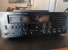
![20251117_180731[1].jpg](https://www.worldwidedx.com/data/attachments/72/72449-42e27768cea99d8e2a9cd691a41050e1.jpg?hash=IkjX9EyRZx "20251117_180731[1].jpg")
")
Yeah, I'm just another dinosaur waiting for the asteroid.Great to know you're all still out there.
Brandon were can I find the full view of this schematic for the 696F base. Looking for it online but have had no luck. Need wiring diagram for the 696F base switch panel wiring. Thanks.First things first. Verify you have 13.8v at the power supply G. If you are using a 12v supply, the numbers in the manual will not be possible.
View attachment 74773
Lets talk about SSB. Since this radio has an automatic power control (instead of just a transistor switch saturating the passthrough regulator), transistor Q56 serves to hold the output at 12.5v.
Lets assume you did have 12.5v at TP7 (A). D103 is a triple-junction diode, so assume it drops .65v * 3 = 1.95v of that. 12.5v - 1.95v = 10.55v at point B. The voltage divider R271 and R270 cut that in half and present 5.275v to the emitter of Q56. Point D is .65v higher at 5.925v. VR17, in combination with the RF Power pot form a voltage divider that sets this base voltage at point D and holds it steady.
Think of Q56 as a voltage comparator. With the base held constant, as RF pulls down on the final supply A, Q56 wants to conduct harder, and this pulls down on the darlington pair (Q54 and Q55) to work to raise that final supply back up. It is a constant battle around that loop to hold A at 12.5v.
The two diodes at F serve to isolate this APC bias voltage from the AM carrier voltage, both of which must share the same RF Power control.
Lets stop there and see if you can figure out why you can't reach 12.5v. If this was too hard to follow, take some voltage measurements at all those points in SSB with no modulation.
 www.manualslib.com
thanks I'll keep that one but I need the 696F base schematic. Putting wiring back to stock on the switch pcb board and someone changed it putting in extra frequencies. So I'm needing the wiring diagram to put the switch panel back to stock.IF it uses the EPT069610Z main board then this should get you close:
Download Galaxy DX 959 Service Manual | ManualsLib
Thank you for your help. The ALC (VR13) has little to no effect (2W max) The APC should be 12.5VDC by the manual I'm using the best it gets to is 12VDC but I wouldn't think 0.5V would make a 10 to 12W difference?
Automatic power control, see post #23. TL-DR it sets the final supply voltage in SSB instead of the easier method of saturating the passthrough for max voltage..What does APC stand for?

![20251117_180354[1].jpg](/data/attachments/72/72450-9bec060d2091c493fdccc843198a7863.jpg?hash=ns58yVA3lJ)
![20251104_132441[1].jpg](/data/attachments/72/72451-734c6779c629a0f94c4cf04cc5c3d7ee.jpg?hash=Zq9_NkIDPS)