Can anyone provide some information on the U1 diodes used across the gates of many newer MOSFET amplifiers? I was told they are a pair of back to back diodes to protect the gate. I would think they would need to be zener diodes due to the voltages present on the gate. Any info would be appreciated.
You are using an out of date browser. It may not display this or other websites correctly.
You should upgrade or use an alternative browser.
You should upgrade or use an alternative browser.
-
You can now help support WorldwideDX when you shop on Amazon at no additional cost to you! Simply follow this Shop on Amazon link first and a portion of any purchase is sent to WorldwideDX to help with site costs.
U1 diodes in MOSFET linears?
- Thread starter Shockwave
- Start date
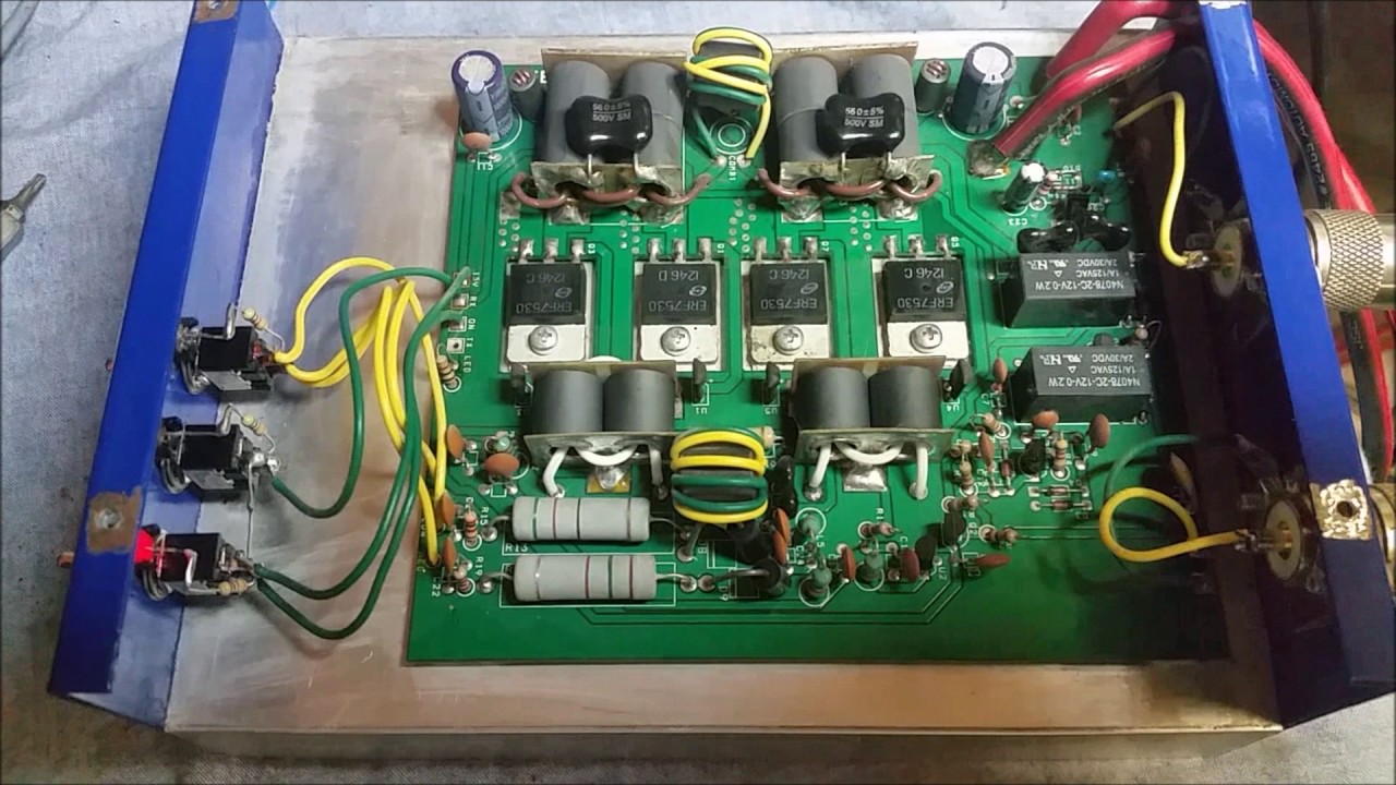
I wish I had a schematic because then I could get a better idea. I do have a link to this picture that shows 4 of them clearly on the board listed as U1 through U4 right above each FET shown here: https://i.ytimg.com/vi/X06a4m5rjXU/maxresdefault.jpg
It seems most manufactures are hiding that these are some diode configuration and I think it protects the gates of the transistors. I think it was on this forum someone said they were a pair of back to back diodes but I don't remember what kind. Any help or some schematics of something similar would be helpful. I'm also wondering about the value of R1 shown in the picture. Does anyone know if they are using 22 ohms here? It's the resistor that brings the center tap of the input transformers to RF ground.
From the picture alone it looks like the diodes conduct if the gates get too much drive, bias or ESD and the value of that resistor is allowing a place for the voltage to drop safely... The resistor value may also alter the gain and drive level requirements. Any thoughts?
Last edited:
http://www.cbtricks.com/miscellaneous/fet_papers/mosfet_experiment.htm
Looks like the biasing devices that RF Limited used to sell.
Looks like the biasing devices that RF Limited used to sell.
Last edited:
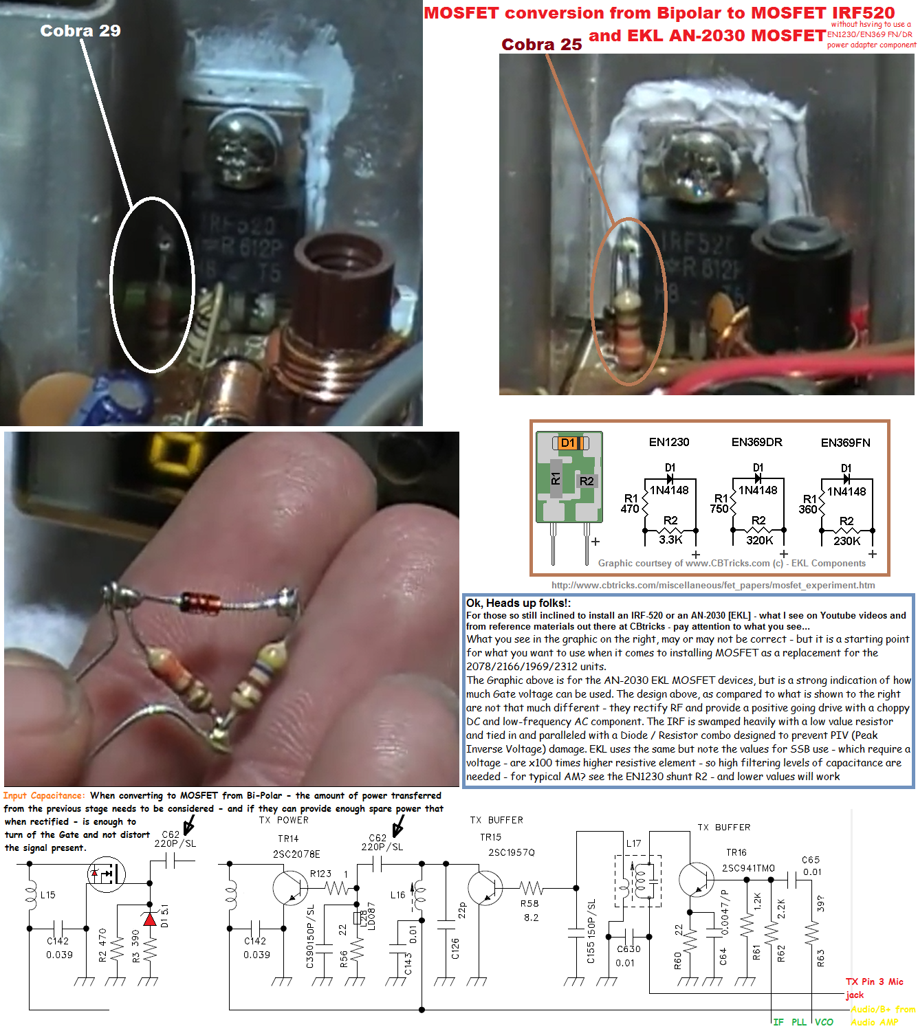
They are the "self-bias" building blocks of the ERF series of MOSFET.
They simply "sample and convert" some of the RF into Rectified DC that allows the Gate to turn on.
The data shown below was from research I did to obtain more information about values used for the IRF520 series. The process is the same, "sample" a small amount (low power) of RF using a method of resistance INTO a gain cell that rectifies the power - this generates a DC value relative to the power coming into the circuit - and due to the GATE's high efficiency high impedance state (it's not a Bipolar that requires power as current in their Base to turn on) the voltage presence helps the Gate in providing the field power as DC to turn on the Drain To Source region of the MOSFET. The Gate simply sees the DC and RF together as a power - and the DC value "pushes" up the Gates turn on value to make it turn on. The DC voltage in this circuit is low-power and hardly any current - just a presence (Think like NEON or Fluorescent light a voltage is needed to start the process and maintain it) that makes the MOSFET turn on and there is just enough power so the RF and it's "waveshape" takes over the gate and the Drain to Source follows the RF wave as a mirroring effect - the DC is not supposed to be too strong and make the Gate "latch" just have enough power to make the part "available" to follow the Input of RF at the Gate and generate output at the Drain To Source Terminals - like a very efficient switch - only very fast. Like Nano seconds - fast.
Last edited:
In another set of posts, I came across a method that many users seem to like better - uses a voltage divider circuit to "feed" the Gate a voltage and keep RF where it belongs - at the Gate.
The method simply uses the TX-side 8V power feed that appears at the Pre-driver as "turn on" for the Collector when you key up - the Transistor senses the Mike keying - so it toggles the power lines to make the TX line like with 8V.
They use this scheme of 8VDC only when TX'ing - so it only makes the Gate turn on when you transmit.
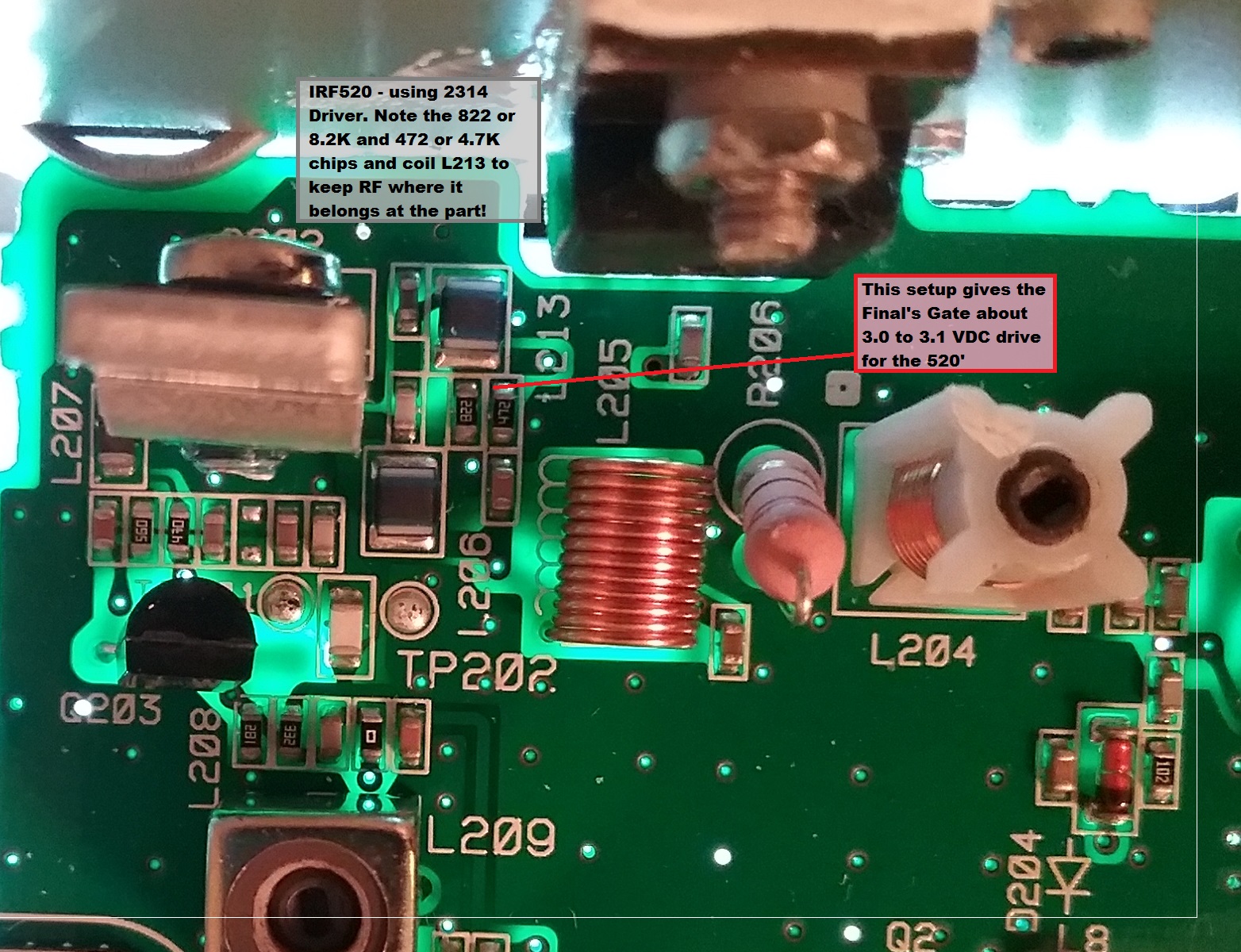
Just like what you did with the U1 or ERF EN-1230 or like what the IRF-520 can utilize ...
The "divider" consists of two resistors to "pare down" the voltage but the circuit is PRELIMINARY - meaning not yet tested in real world applications only theoretical...
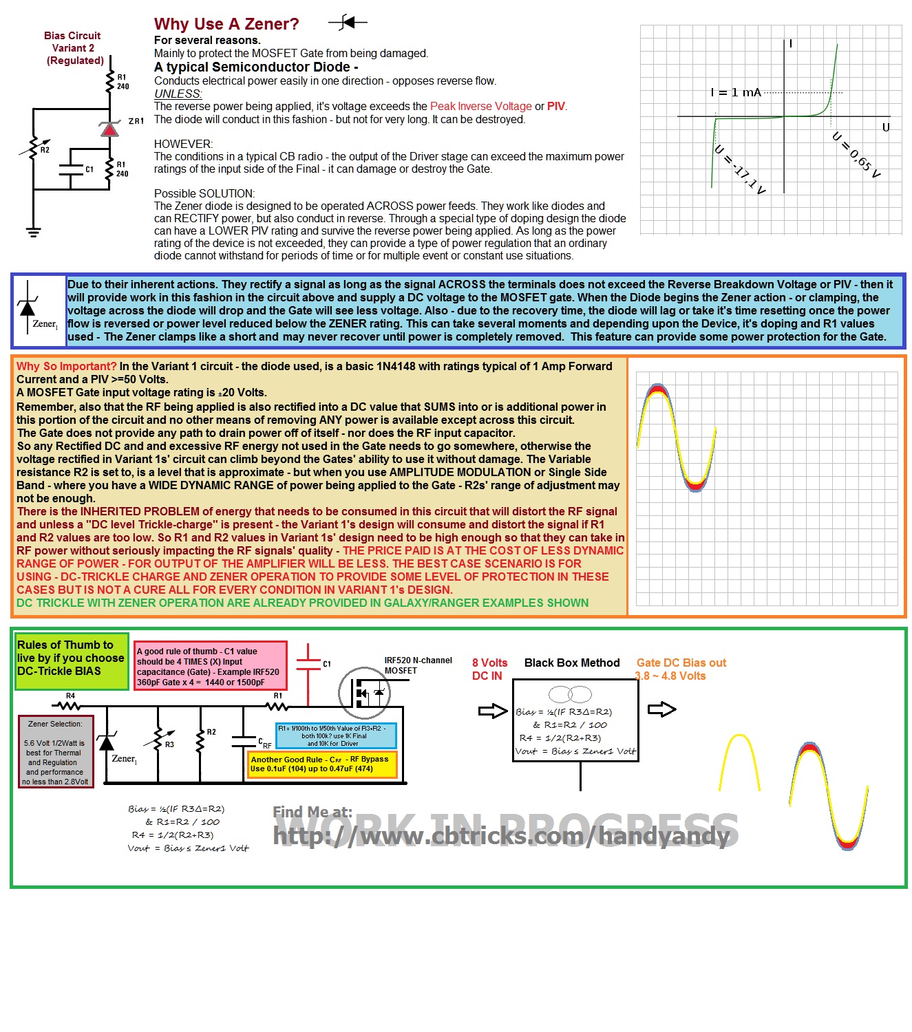
Use at your own risk - but it can provide a study for you to engage your efforts.
The above is also similar to BIAS circuits commonly used in todays SSB radios that require a constant current supply of a very low voltage but a good amount of current, across a diode that is physically attached and can thermally track the part is designed to bias for - properly, so it can stay in it's Class of operation like Class AB.
MOSFET design like this utilizes the BIAS but only as a means to make the Gate region turn on and track RF properly without adding distortion.
Again I caution you, this is a work in progress that someday may be completed but is inconsequential if not utilized. It is only for educational purposes.
The method simply uses the TX-side 8V power feed that appears at the Pre-driver as "turn on" for the Collector when you key up - the Transistor senses the Mike keying - so it toggles the power lines to make the TX line like with 8V.
They use this scheme of 8VDC only when TX'ing - so it only makes the Gate turn on when you transmit.
Just like what you did with the U1 or ERF EN-1230 or like what the IRF-520 can utilize ...
The "divider" consists of two resistors to "pare down" the voltage but the circuit is PRELIMINARY - meaning not yet tested in real world applications only theoretical...
Use at your own risk - but it can provide a study for you to engage your efforts.
The above is also similar to BIAS circuits commonly used in todays SSB radios that require a constant current supply of a very low voltage but a good amount of current, across a diode that is physically attached and can thermally track the part is designed to bias for - properly, so it can stay in it's Class of operation like Class AB.
MOSFET design like this utilizes the BIAS but only as a means to make the Gate region turn on and track RF properly without adding distortion.
Again I caution you, this is a work in progress that someday may be completed but is inconsequential if not utilized. It is only for educational purposes.
Attachments
Thanks for that info and the schematic of the EN part numbers. While the circuit used to replace finals in radios is self bias because those AM radios didn't have bias, I suspect the ERF7535 in the pictured amp uses regulated bias. If you look at the part they are calling U1, it looks like a 3 terminal regulator. The ground and output pins are also in the right spot. I think it's a small TO-92 packaged 7805 regulator. I'm very interested in what value that R1 is on the back of the input transformers. Also, if anyone knows what one of the three EN parts works well with the EFR7535 final, please tell. Probably the one with the lower value resistors but that's just my guess.
I'm off topic here guys and not trying to get into the mix.
I just always post this thread whenever i see the 'homebrew bias parts' from CBtricks being posted:
https://www.worldwidedx.com/threads...rawing-and-the-correction.157713/#post-436556
the 369FN has a typo and will not work correctly as it is drawn.
and im back out.
LC
I just always post this thread whenever i see the 'homebrew bias parts' from CBtricks being posted:
https://www.worldwidedx.com/threads...rawing-and-the-correction.157713/#post-436556
the 369FN has a typo and will not work correctly as it is drawn.
and im back out.
LC
just so i can add to the actual topic, here is a pic of a Palomar 450 FET amp that should provide some enlightenment:

U1 looks like an EN1230 to me.
LC

U1 looks like an EN1230 to me.
LC
Sorry LC I made a mistake on what looks like the 3 pin regulator number. It is not U1, it is U7 and is in the bottom right corner of the pic I posted. It's behind the input transformers. Still looking for info regarding R1 which is just above and to the right of the U7.just so i can add to the actual topic, here is a pic of a Palomar 450 FET amp that should provide some enlightenment:

U1 looks like an EN1230 to me.
LC
Update: I found the resistor value and the regulator in this schematic:
http://www.cbtricks.com/Amp/palomar_other/palomar_hd_450_fet/graphics/palomar_hd_450fet_sch.pdf
I kind of expected the regulator to be 5 volts but that R1 at 1000 ohms was a surprise. That's much different than what we would see with bipolar transistors.
http://www.cbtricks.com/Amp/palomar_other/palomar_hd_450_fet/graphics/palomar_hd_450fet_sch.pdf
I kind of expected the regulator to be 5 volts but that R1 at 1000 ohms was a surprise. That's much different than what we would see with bipolar transistors.
Hmmm. Using 16v caps? Ya think they would have chosen at least 25v for the build. Cheap caps as well doesn't inspire confidence. Just saying.
shockwave, im glad to see you found the info you were looking for.
I do wonder if you meant 10K for R1 in that schematic though, as that's what i see there.
LC
I do wonder if you meant 10K for R1 in that schematic though, as that's what i see there.
LC
Just remember that the 1230 can also be used as a "Stand alone" to power the Gate - you adjust the capacitance into the circuit to apply enough drive - it will do the rest.
So in reference to the Palomar, that 1K is simple current limiting - the Gate's can rise to as high as 7 volts DC crudely measured while it's powered up using a Dead Carrier of about 4 watts. They say they can handle up to 20VDC on the gate so --- Go For Broke - eh?
The easier way to see it's "Shunt resistor" is to simply DVM the ohmic results - both ways, one will be quite low - with Diode resistor in parallel but reversed test lead (polarity reversed) the ohmic reading can be made DIRECT.
They have changed to LOWER values...while they were being made thru the years...So when CBT first posted those results - not everyone saw these values - but then too, capacitor values were modified thru the years as they (Read:EKL) refined the balance.
Look for Motorolas' 12N10 (not the 13)...you'll get a clue there too...(Hint: Fig. 5)
The one observation I have to offer is their capacitive levels. Although sluggish compared to say a 13N10 - they operate under a similar principle of using input capacitance TO the Gate and the Gates' OWN capacitance - put the two together - forms a Paralleled capacitance circuit - you can use these crude values as a means to "cushion" and shape the RF wave to offset any sort of skewing the DC bias will bring to the table due to it's own rectification - per the EN1230 or 369FN/DR parts. A power level value can be obtained from that to keep the RF wave symmetry even and not skewed.
ADDED---:
To add a little more, the Fig 5 in the PDF, is for demonstration of how the Gate charge changes.
So there too is another event like paralleled - in series related to capacitance - or why the Gate has a capacitance and how to offset it's input capacitance with the proper level of drive, either by DC offset (raise or lower trigger) or adjust input capacitance to offset the power losses incurred by the device (in this scenario ERF types) having to absorb and convert RF value to a DC value - and to use the EN 1230 as a stand alone is possible - but take heed that as you raise the Drive Resistance in using the 1230 from <1K to a higher value towards 10K it takes a lot longer to remove the field charge from the Gate simply due to the effort the voltage has to drop across the ERF device (reverse bias on diode as well) to take longer to drain away- so lead dress as well as the shortcomings of higher "Bleed down" voltage presence may make the parts "latch" and stay latched if you want to raise that Gate Bias voltage too high.
A secondary event of oscillation is going to occur if the Gate charge "spills out" and the Resistors cannot keep the Charge contained . There is a reason for that 5V regulator and it's RF bypass - it helps act as a shock absorber when Gate voltage RISES above 5V - the Feed rises too and the Regulators own sense will work around this - but only to a certain degree.
Think of the 5V and it's purity as a "baffle" in that reserve pool - too many waves create the turbulence - while the Baffle that regulation provides, lends to tamping it down.
IF any of you know of Hot Spotting - this is what could happen to that Gate region. So to "Choke off" the feeder and leave the 1230 to fend for itself - it may need more help in the use of extra swamping resistance to stabilize the gate and provide a path for the charge to escape or at least stabilize.
Some radios, including Uniden are using a similar method ...
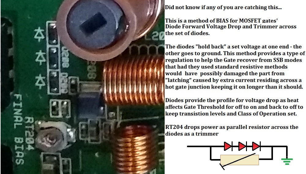
Just cautioning the rest of you so you don't suffer that same fate as I did learning the above lesson.
So in reference to the Palomar, that 1K is simple current limiting - the Gate's can rise to as high as 7 volts DC crudely measured while it's powered up using a Dead Carrier of about 4 watts. They say they can handle up to 20VDC on the gate so --- Go For Broke - eh?
The easier way to see it's "Shunt resistor" is to simply DVM the ohmic results - both ways, one will be quite low - with Diode resistor in parallel but reversed test lead (polarity reversed) the ohmic reading can be made DIRECT.
They have changed to LOWER values...while they were being made thru the years...So when CBT first posted those results - not everyone saw these values - but then too, capacitor values were modified thru the years as they (Read:EKL) refined the balance.
- NOTE: "refined" may imply an "error" - not really, MOSFET refinements thru the years provided various ways to get the power thru the device so as the playing field grew, so did it's grass - and required mowing eliminated a lot of weeds but then took away some of the better turf they used to obtain their drive and performance they are so noted for.
Look for Motorolas' 12N10 (not the 13)...you'll get a clue there too...(Hint: Fig. 5)
The one observation I have to offer is their capacitive levels. Although sluggish compared to say a 13N10 - they operate under a similar principle of using input capacitance TO the Gate and the Gates' OWN capacitance - put the two together - forms a Paralleled capacitance circuit - you can use these crude values as a means to "cushion" and shape the RF wave to offset any sort of skewing the DC bias will bring to the table due to it's own rectification - per the EN1230 or 369FN/DR parts. A power level value can be obtained from that to keep the RF wave symmetry even and not skewed.
ADDED---:
To add a little more, the Fig 5 in the PDF, is for demonstration of how the Gate charge changes.
So there too is another event like paralleled - in series related to capacitance - or why the Gate has a capacitance and how to offset it's input capacitance with the proper level of drive, either by DC offset (raise or lower trigger) or adjust input capacitance to offset the power losses incurred by the device (in this scenario ERF types) having to absorb and convert RF value to a DC value - and to use the EN 1230 as a stand alone is possible - but take heed that as you raise the Drive Resistance in using the 1230 from <1K to a higher value towards 10K it takes a lot longer to remove the field charge from the Gate simply due to the effort the voltage has to drop across the ERF device (reverse bias on diode as well) to take longer to drain away- so lead dress as well as the shortcomings of higher "Bleed down" voltage presence may make the parts "latch" and stay latched if you want to raise that Gate Bias voltage too high.
A secondary event of oscillation is going to occur if the Gate charge "spills out" and the Resistors cannot keep the Charge contained . There is a reason for that 5V regulator and it's RF bypass - it helps act as a shock absorber when Gate voltage RISES above 5V - the Feed rises too and the Regulators own sense will work around this - but only to a certain degree.
Think of the 5V and it's purity as a "baffle" in that reserve pool - too many waves create the turbulence - while the Baffle that regulation provides, lends to tamping it down.
IF any of you know of Hot Spotting - this is what could happen to that Gate region. So to "Choke off" the feeder and leave the 1230 to fend for itself - it may need more help in the use of extra swamping resistance to stabilize the gate and provide a path for the charge to escape or at least stabilize.
Some radios, including Uniden are using a similar method ...
Just cautioning the rest of you so you don't suffer that same fate as I did learning the above lesson.
Attachments
Last edited:
LC, I think I'm past the point where I need glasses the way I'm messing up these part numbers. It was not R1 I tried to describe. It's R3 and R11 on the center tap of the input transformers. Sorry for the confusion and thanks for everyone's help.shockwave, im glad to see you found the info you were looking for.
I do wonder if you meant 10K for R1 in that schematic though, as that's what i see there.
LC
dxChat
- No one is chatting at the moment.

