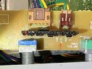
Here is the schematic to it from a 949

As you can see, this is much like a clipper circuit - So if you're having issues - might want to just bypass this circuit - I know it seems to be a lot to sacrifice for a means to reduce noise, but the basic premise of this is to purposely overamplify the signal - then filter the signal to narrow it's bandpass - extremely - then with all the amplified vocal range - REDUCE or attenuate the signal back down to low-level input. Supposedly this process leaves you with vocal range audio of the noisy signal - in hopes you hear the voices embedded in the noise it tries to filter out.
Ok, so why doesn't it work?
Several reasons, one main one is already brought up - the header to the main board may have been installed in reverse. So it doesn't turn on - doesn't do anything - but what it is supposed to do, when it is not on? It is to be bypassed.
But it needs power to do that - so it is supplied by the B+ feed. ANF is a toggle function - it sends power to the board. So if the header isn't set up right - you hear nothing. But since you need it to be on in order to hear - you may want to try and bypass the board fully; by shorting the I/P (Input Port) to O/P and leave it alone - then it may indicate you have a bad ANF/GNF switch. which may need further diagnostics and see if the SMD IC is even working.
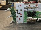
So it may be easier to unsolder the board then re-routing audio thru as a bypass jumper across two pins.
It's is done by shorting Pin 2 to Pin 4 - see below

The reason why I mention to just remove it, is due to the
inability to provide a simple fix for a board that is a noise filter / clipper.
The level of diagnostics would require more tools than may have available.
How does it do that?
When ANF is on - Q302 - a Darlington switch - is powered on, by a positive signal to the Base of Q302 - doing that, it pulls away power from R320 - a buffer resistor for a directional audio switch - D301 and also it simply biases the input (of the 1st stage output) to 1/2 value - further reducing amplification of that signal arriving from I/P. This is so the signal peaks can be found and filtered.
What is going on - setting ANF line low (GNF off) it is using D301 in a function much like an RF switch, it passes Audio sensed from the 1st stage and simply sends it thru to Q301 - set up as a buffer amp - looks at the output of IC1-C and everything else is ignored. ANF/GNF off - your bypass.
How? By D301 - by having a 2nd diode - When GNF of OFF now placed in reverse bias - turning off the output (by swamping) IC1-B using DC to "quench it". Power applied to the diode - is slowed down by the 15K resistor R317 - which raises the voltage in the line which then forces more power from the audio peaks to pass thru the switch. This DC level sinks into IC1C's output - it reflects this lines output at IC1C Pin 8 - so the diode allows the signal to pass. But due to the higher voltage presence - the output of IC1B Pin 7 is swamped out the Diode is keeping the ability of Pin 7 to send any signal - even though it can though it being "forward biased" if the output of that Pin was strong enough - in a way - this circuit works a lot like squelch control - it only lets audio pass if the signal can force it's way thru a DC bias presence.
This is how the biasing of MOSFET and Bipolars work - and why so little current is needed for the higher Gate voltage (MOSFET) or for the low voltage but higher current to a limit in Bipolars...as long as the signal is strong enough to overcome the voltage and power presences (as a varying value working against an impedance) in the line to the Base (bipolar) or Gate (MOSFET) the signal can supplant and augment the bias and become a working value to develop output across the output terminals.
When ANF in "enabled" that is done by supplying power (to that ON pin) to "turn off" a power feed that would otherwise go to the Directional Audio Switch Q302 passes all the power from the 8V+ feeder into ground - it's pulled from power dropped by R320 - that would otherwise power the D301. So when power is applied to the ON pin, that turns on the Transistor like a switch puts power - thru itself, to ground. Turning off this system - by using starvation - D301 then only has little function except to act like a clipper to the signal.
The IC is still on, but follow the traces, IC1C Pin 8 is the "source" for the Diode switch D301 - to hear the audio.
- With GNF off let's power flow into D301 and into R317 - in applying power, Pin 8 sinks power from R317 - but power in the line also goes to IC1D Pin 12. The non-inverting input - turns it on like a switch - non linear function (it is also why it uses capacitors in the feedback - block DC but pass audio) So this section of the amp is turned off - by swamping a pin to keep it high.
So when you turn on Q302 - the transistor sinks the power going to D301 and that 15K resistor - allowing the Diode to work as a clipper, directional switch (PIN diode function) is off and audio passes to Q301 thru D301 from IC1B Pin 7.
Positive peaks occurring flow thru D301 and by following the power flow - any negative peaks are trimmed to ground filtered thru C312 (0.033uF Chip) while positive peaks as well as what is left - are allowed to go into Q301 buffer amp thru "vocal range pass filter" series circuit R321 and C316 - everything produced and processed thru IC1-C thru IC-1B (D and A are filter networks) are allowed thru D301 into Q301 and out thru the O/P (Output Port).
I just don't want to lead you down a rabbit hole that can otherwise be avoided and more of your time spent enjoying the hobby even though the board is potentially repairable - the SMD parts and the board itself are too delicate for most typical hobby soldering irons. IT can destroy the board using too much heat on the small parts and the foil traces.